AKESO ntnb
Agile Micro-Fabrication Foundry
Beijing / Zhenjiang, China
Planet Earth
An interdisciplinary vocational guild for photon architects. Every day we practice the craft of simulation, lithography, and characterizing metasurfaces and optical devices—from Maxwell's equations to atomic precision.
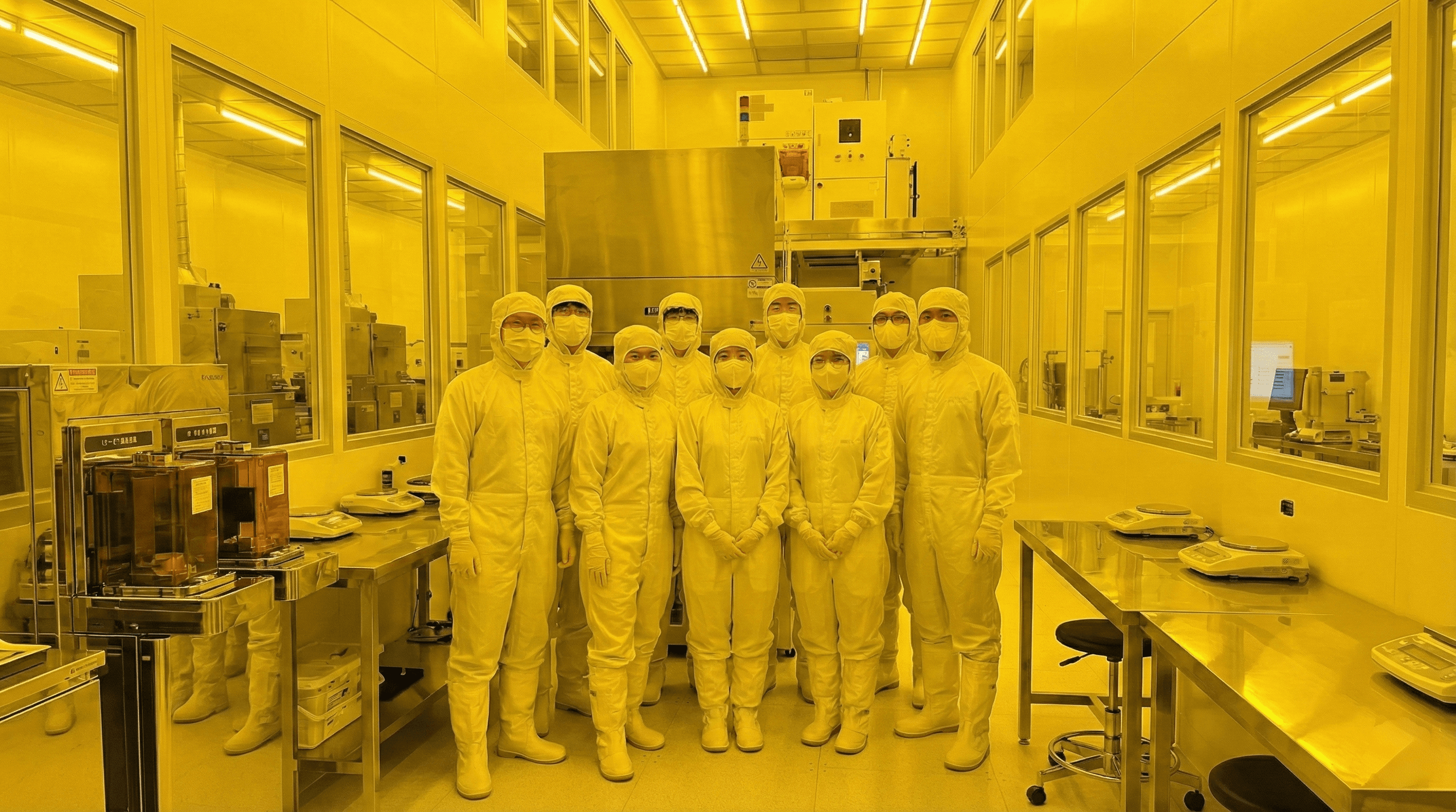
We provide a dedicated R&D tiger team to turn your optical concepts into physical reality.
That team is a 7-person cross-disciplinary unit specializing in nanophotonics, computational physics, material science, and cleanroom processes. Unlike traditional large-scale fabs that are rigid and slow, we operate an in-house agile micro-fab.
We specialize in Metasurface Optics (Metalens, DOE, AR/VR Waveguides), covering the full spectrum from FDTD simulation, layout design, to EBL/Photolithography, etching, and coating. We bridge the "Valley of Death" between academic papers and mass production prototypes.
RESOURCES
Technical Downloads
Design Rules Manual
Complete fabrication constraints & DRC specs
Brand Logo
Official AKESO ntnb vector logo for co-branding
GDSII Layer Properties
KLayout layer colors & styles
Layer Mapping Table
GDSII layer/datatype definitions
Copyright © 2026 AKESO ntnb. All rights reserved.